What is Advanced Packaging and Chiplet Design?
Advanced Packaging and Chiplet Design Training
Advanced Packaging and Chiplet Design certificate program provides a comprehensive, hands-on pathway to mastering the semiconductor industry’s most transformative frontier. Designed for IC designers, packaging engineers, system architects, and technical managers, this training bridges the gap between traditional monolithic chips and the heterogeneous integration era. By the end, participants will be able to evaluate packaging technology trade-offs, partition systems into chiplets, and drive co-design decisions that directly impact performance, yield, and time-to-market.
The program progresses from foundational substrate and interconnect principles through advanced 2.5D interposers, 3D die stacking, hybrid bonding, and fan-out panel-level methods, then deepens into chiplet partitioning, die-to-die standards like UCIe, power delivery, thermal management, signal integrity, and reliability testing. Each lesson balances theoretical frameworks with real-world case studies, building four core skill areas: packaging architecture selection, chiplet system design, electrical and thermal co-design, and advanced testing strategies. With the industry racing toward chiplets for AI, HPC, and mobile applications, this training equips you to lead in a landscape where packaging innovation now defines system-level performance—making this the ideal moment to invest in these critical skills.
What is Advanced Packaging and Chiplet Design?
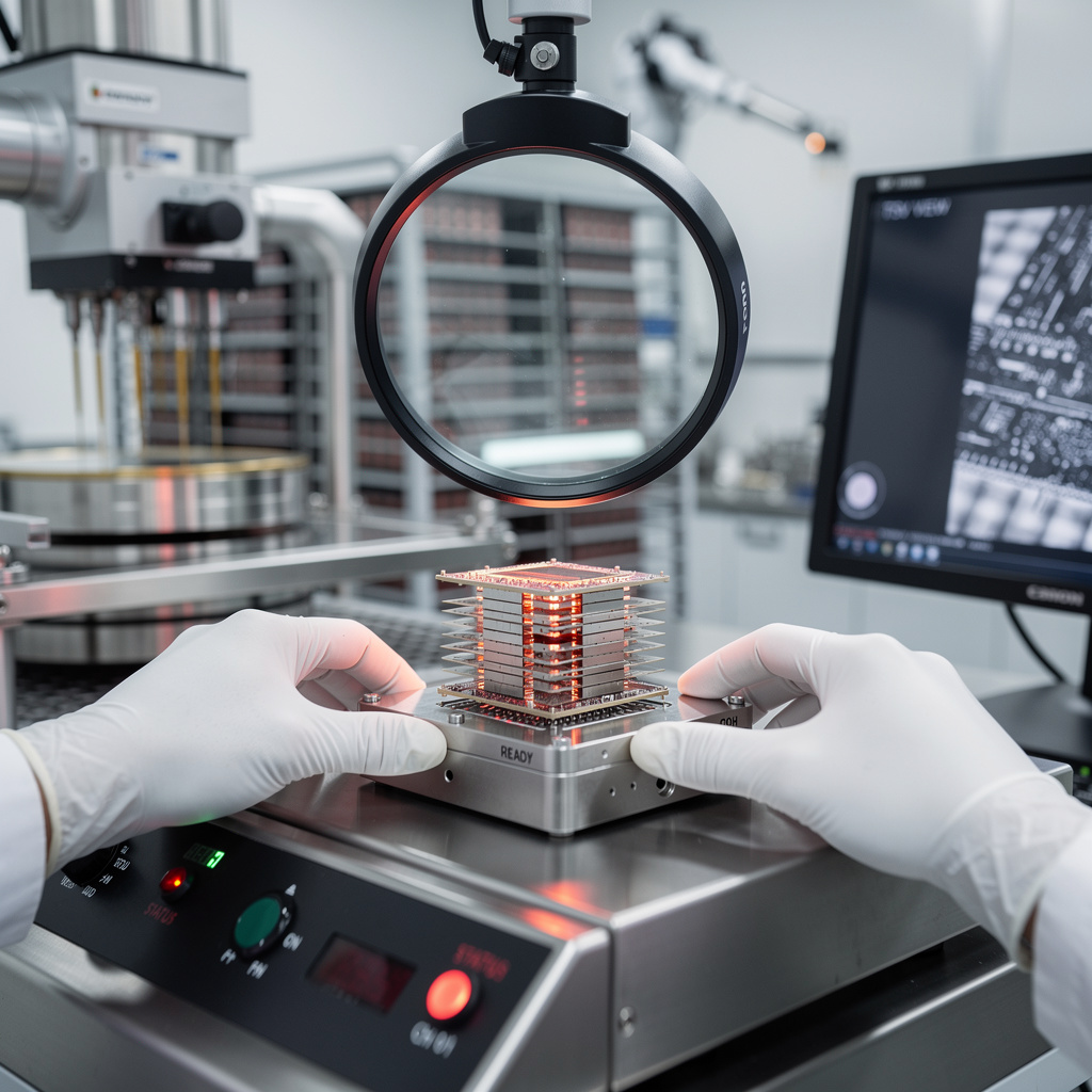
Advanced packaging and chiplet design is the discipline of integrating multiple silicon dies—often heterogeneous in function, process node, or vendor—into a single, high-performance system using sophisticated interconnect and assembly technologies. Core concepts include 2.5D integration with silicon or organic interposers, 3D die stacking with through-silicon vias and hybrid bonding, fan-out wafer-level packaging, and the partitioning of a system into smaller chiplets connected via standardized die-to-die interfaces. This field redefines how computing systems are built, moving beyond the limits of monolithic scaling by enabling modular, reusable, and cost-effective system-on-package solutions.
Today, advanced packaging is the primary driver of continued performance gains in AI accelerators, data-center CPUs, GPUs, and edge devices, as traditional Moore’s law scaling slows. Industry leaders like TSMC, Intel, and Samsung have made packaging a strategic pillar, while standards such as UCIe and chiplet ecosystems from multiple vendors are reshaping supply chains and design methodologies. Real-world applications range from high-bandwidth memory stacks and photonic co-packaging to automotive and 5G/6G systems, where power efficiency, signal integrity, and thermal management are critical. The recent shift toward panel-level processing and hybrid bonding further underscores how packaging innovation now determines system-level speed, density, and energy efficiency.
Mastering this subject builds a unique skill stack that combines electrical engineering, materials science, mechanical/thermal analysis, and system architecture. Professionals who understand advanced packaging can optimize chiplet partitioning, select appropriate interconnect schemes, manage crosstalk and power delivery, and ensure reliability through known-good-die strategies and advanced testing. This expertise is invaluable for roles in semiconductor design houses, foundries, OSATs, and system integrators, as well as for researchers exploring emerging technologies like chiplets for quantum or neuromorphic computing. The ability to navigate this interdisciplinary domain empowers engineers to make strategic decisions that directly influence product performance, cost, and scalability—making it a cornerstone of modern electronics innovation.
Common Questions About Advanced Packaging and Chiplet Design
How does the Advanced Packaging certificate boost a chip design resume?
Can beginners with no packaging experience join the Advanced Packaging course?
Why is ABF substrate crucial for high-performance advanced packaging?
How does hybrid bonding achieve sub-micron pitch in 3D die stacking?
What are the key trade-offs between TSV and RDL in interposer design?
How does chiplet partitioning improve yield beyond the reticle limit?
- Smaller die area reduces the chance of a random defect landing on the die.
- Known good die testing allows only functional chiplets to be assembled, avoiding waste.
Is advanced packaging just a stopgap until Moore's law fully ends?
What Will This Course Bring You?
- Analyze the drivers and landscape of advanced packaging to identify market trends and technology roadmaps.
- Design a 2.5D integration solution using interposers to optimize interconnect density and performance.
- Evaluate hybrid bonding techniques for 3D die stacking to achieve fine-pitch interconnects.
- Apply fan-out and panel-level packaging methods to reduce cost and form factor for heterogeneous integration.
- Implement chiplet partitioning strategies to balance performance, yield, and cost in system design.
- Compare die-to-die interface standards such as UCIe and BoW to select appropriate protocols for chiplet communication.
- Analyze power delivery and thermal management challenges in advanced packages and propose mitigation techniques.
- Apply design tools and co-design methodologies to integrate electrical, thermal, and mechanical aspects of advanced packaging.
Curriculum
12 Units1. Drivers and Landscape of Advanced Packaging
1 hour
2. Substrates, Interconnects, and Assembly Basics
1 hour
3. 5D Integration with Interposers
1 hour
4. 3D Die Stacking and Hybrid Bonding
1 hour
5. Fan-Out and Panel-Level Packaging
1 hour
6. Chiplet Partitioning and System Design
1 hour
7. Die-to-Die Interfaces and Standards
1 hour
8. Power Delivery and Thermal Management
1 hour
9. Signal Integrity and Crosstalk Control
1 hour
10. Design Tools and Co-Design Methodologies
1 hour
11. Testing, Known Good Die, and Reliability
1 hour
12. Emerging Technologies and Future Directions
1 hour
Exam – Advanced Packaging and Chiplet Design
20 Questions • 70% Pass • 30 min
Unlock All Units for Free
Create an account, enroll in the course, and start with the first unit right away.
Exam – Advanced Packaging and Chiplet Design
20 Questions • Pass: 70% • 30 min
Course Duration
720
Total Minutes
12
Unit
1
Final Exam
~60
Min / Unit
Advanced Packaging and Chiplet Design Certificate Program
Document Your Skill
Those who pass the 20-question, 30-minute exam with 70% receive the Advanced Packaging and Chiplet Design Certificate.
Stand Out on Your CV
By adding your certificate to your CV, gain a professional reference in job applications and stand out from the crowd.
Career Advantage
Catch Wisdom certificates are recognized by HR departments and increase career opportunities.
CERTIFICATE FEE
At the end of the course, an online exam consisting of 20 questions with a 30-minute time limit is given. The exam appears automatically after you complete the topics. Anyone who scores at least 70 out of 100 on the certificate exam is awarded the Advanced Packaging and Chiplet Design Document (certificate of attendance). You can add the certificate you earn to your CV for job applications in the many sectors listed above, and use it as a reference proving that you took this interactive course.
The Certificate of Achievement you receive with the Advanced Packaging and Chiplet Design course program holds value that proves your personal and professional development in the business world. By adding it to your CV, it can serve as an important reference in your job applications. Moreover, compared with certificates from other private training institutions, Catch Wisdom certificates are offered to our participants at a much more affordable price.
Because HR departments recognize Catch Wisdom as a reputable institution in this field, they value these certificates and may evaluate your job applications favorably. For this reason, a Advanced Packaging and Chiplet Design course certificate from Catch Wisdom can make your applications more attractive and place you in an advantageous position in the business world.
For more information, we recommend visiting the Support page.
Certificate in 7 Languages
Earning success certificates from our courses is now more meaningful and global. With certificates available in Turkish, English, German, French, Spanish, Arabic, and Russian, we fully unlock the potential of students worldwide.
Why Certificate in 7 Languages?
-
01
Global Skill Development
Receiving your certificates in 7 different languages strengthens your communication skills as you engage with more people worldwide. It lets you operate more confidently and capably on the international stage.
-
02
International Job Opportunities
Employers may see your certificates in multiple languages as a sign of your ability to seize global opportunities. You can open more doors to new jobs and projects.
-
03
Cultural Richness
The chance to earn certificates in different languages helps you build closer ties with various cultures and broadens your worldview. It enriches your global perspective and deepens cultural understanding.
-
04
Ability to Participate in International Projects
Multilingual certificates give you an edge to work more effectively on international projects. They boost your chances of leadership and participation in diverse projects in the business world.
-
05
Prove Yourself on the Global Stage
Certificates in multiple languages let you showcase your skills and knowledge worldwide. You can become an internationally recognized professional.
Language diversity opens worldwide opportunities. If you want to prove yourself in the international arena, join our online Advanced Packaging and Chiplet Design course program and begin this journey with us.
Frequently Asked Questions (FAQ)
Is this course paid?
How do I join the course?
Can I take the course at my own pace?
How can I get my certificate?
What are the advantages of the Certified Certificate?
Boost Your Career
Take a new career step with the Advanced Packaging and Chiplet Design course. Add your certificate to your CV, stand out in job applications, and open the door to new opportunities in the industry.
StartStudent Reviews
No reviews yet
Enroll in this course and be the first to leave a review about your experience with Advanced Packaging and Chiplet Design.
Start